
ORLANDO, Fla. — As artificial intelligence drives demand for more powerful chips, semiconductor manufacturers are paying closer attention to the smallest steps in the production process.
One of those steps is chemical-mechanical polishing, often called CMP. The process is used to smooth and prepare wafer surfaces during chip manufacturing. If it is not carefully controlled, tiny defects can affect chip performance, reliability and manufacturing yield.
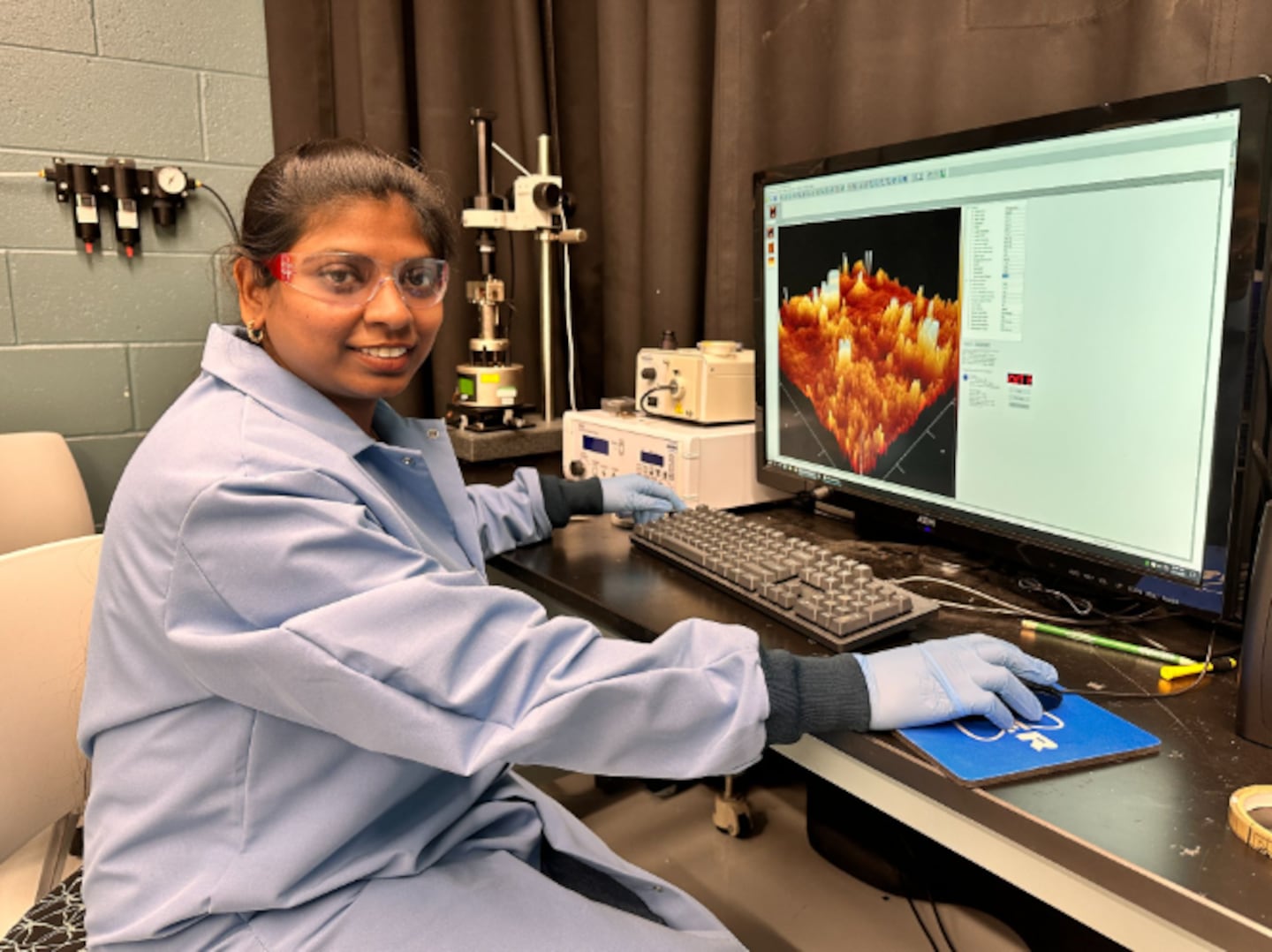
Dr. Harini Bhuvaneswari Gunasekaran, a postdoctoral researcher at Clarkson University, has worked on a particle-free polishing system designed to reduce defects during a sensitive stage of semiconductor manufacturing.
Her research focuses on a problem that can occur when copper and tantalum are exposed during polishing. When the two materials interact in that environment, they can create an electrochemical reaction known as galvanic corrosion.
In simple terms, that reaction can cause copper to dissolve more quickly than intended. The result can be surface damage, higher defect rates and reliability concerns for the tiny connections that help chips function.
Traditional CMP processes often use liquid slurries containing abrasive particles. Those particles help remove material, but they can also create scratches, contamination or residue that requires additional cleaning.
Gunasekaran’s work takes a different approach. Her system combines a specially designed polyurethane polishing pad with a particle-free polishing fluid. The goal is to reduce corrosion while avoiding some of the defect risks that can come from abrasive particles.
The polishing pad is designed with chemical groups built into the material itself. Because those groups are bonded into the polyurethane structure, they are intended to remain more stable during polishing instead of washing away or adding unwanted variation to the process.
The particle-free fluid is designed to help control the electrochemical environment between copper and tantalum. Together, the pad and fluid are meant to provide both polishing action and corrosion control without relying on abrasive particles.
For chipmakers, that kind of process control matters because advanced chips depend on extremely small and reliable structures. As the number of connections and interfaces inside chips increases, small defects can become larger manufacturing and reliability concerns.
The issue is especially relevant for AI hardware. Advanced packaging and chiplet-based designs are being used to connect different components more closely and improve performance. But as those systems become more dense, manufacturers need processes that can protect reliability at the materials level.
As semiconductor companies scale production for AI, high-performance computing and advanced packaging, process reliability is likely to become even more important. Improvements at one manufacturing step can affect yield, cost and long-term device performance.
Gunasekaran has presented related work on advanced packaging reliability and interfacial electrochemistry at materials research conferences. Her work points to a broader industry focus on improving semiconductor manufacturing from the materials level up.
For chipmakers, the future of AI hardware will not depend only on better designs. It will also depend on manufacturing methods that can produce those designs reliably at scale.
Click here to download our free news, weather and smart TV apps. And click here to stream Channel 9 Eyewitness News live.

©2026 Cox Media Group


